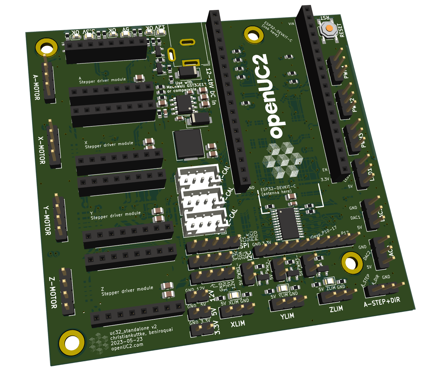
UC2 Standalone Board V3
🔌 Board layout and schematics (UC2 Standalon v3)
The board comes with 4 motor controllers (e.g. A4988 Bipolar Stepper controller or TMC drivers with pololu pinout), the ESP32 Dev Kit, a bunch of pins for in/outgoing connections, 3 darlington transistors (BD809) and the power distribution. It is inspired by the CNC shield and can
- run up to 4 steppers
- run multiple high power LEDs
- be controlled via PS3/PS4 Controllers
- drive Adafruits Neopixels
- trigger a Camera
- provide scanning patterns for Galvos
- control/readout external devices using I2C
We use the ESP32 in order to ensure connectivity via
- Wifi
- Bluetooth
- USB Serial (mostly used)
UC32_standalone
Current revision is "v2" dated 2023-05-23.
The following documents can also help understand how everything is connected:
In the ´kicad´ folder, in the folder for ´esp32_standalone´, in the ´OUTPUTS/for-humans´ folder:
- Schematic PDF (ESP32-cnc.pdf) is a diagram that shows all electronic components, how everything is connected and features part numbers and notes on capabilities.
- Interactive HTML Bill-of-materials (ibom.html) shows a view of the circuit board and a list of the electronic components. Tracks can also be selected to highlight them and see where they go on the actual circuit board.
On the board there are test-pads that can be probed or soldered to. This helps taking measurements of specific circuits and they can be used to modify the circuits, for example by soldering a wire between test points and cutting the trace on the circuit board. The test points are named in the schematic and in silkscreen. The traces can be followed in the ibom.
TODO in this README
- add photos of board and features
- pin assignment of headers and connectors
- add errata section for next revision: endstop pinout ist nicht standard kaufbar
Table of Contents
- UC32_standalone
- TODO in this README
- Table of Contents
- Insertable modules and sub-boards
- Power input and output
- Pinout list
- Headers and connectors
- Reset button
- Errata and notes for the next revision of the board
Insertable modules and sub-boards
ESP32 DEVKIT C (U101)
The ESP32 DEVKIT C is the standard module available from ESP and third parties.
- It has 2 male pin header rows of 19 pins each.
- Micro USB port to supply power and connect to on-board USB to serial converter (CP2102) for programming the ESP32.
- Can be powered by USB or through the UC32_stanadlone's 12V DC input.
- Voltage down-regulator AMS1117 accepts 5V from USB or VIN pin and converts it to 3.3V needed by the ESP32 module. 3.3V is output on 3V3 pin.
- On-board Wifi and Bluetooth antenna
4 Stepper driver modules (J201+J202, J301+J302, J401+402, J501+502)
Four stepper driver modules can be inserted into uc32_standalone. They can be controlled by the ESP32 and the pin headers can be connected to stepper motors.
In the schematic, "stepperdriveboardheaders" and "sdbh" pages are 2 separate header rows designed to fit in a module with 2 male header rows of 8 pins each.
Compatible boards are generic A4988 boards and silentstepstick. The pinout is: looking at the stepper driver module from the side that is toward the uc32_standalone (bottom side):
| Left Row | Right Row |
|---|---|
| Direction | GND |
| STEP | VDD |
| nSLEEP | 1B |
| nRESET | 1A |
| MS3 | 2A |
| MS2 | 2B |
| MS1 | GND |
| nENABLE | VMOT |
- UC32_standalone connects VMOT to 12V and has 44 uF suppository capacitors for the motor current.
- VDD supplied by uc32_standalone is 3.3V
- MS1-3 are pulled to 3.3V over JP103,JP105,JP107 cuttable solder-jumpers placed on the underside of the uc32_standalone board. They are normally closed, can be cut with a knife, and then solder-bridged back closed.
- The module's motor outputs go directly to the motor pins without protection
The modules should be plugged into ESP32_standalone so that the VMOT pin faces the corner of the DAC2 header. Each header for stepper drivers has big capacitors close to that pin.
Power input and output
Power indicator and voltage-OK LEDs
Next to the barrel jack are 3 pairs of LEDs labeled with the 3 different voltages.
The red LED will light if any voltage is present on this voltage's net. The green LEDs indicate that the voltage is correct as expected. When the green LEDs flicker or do not light, then there is undervoltage or a brown-out on that net.
12V
- input
- DC barrel jack type P1J: OD 5.5 mm, hole for pin with ID 2.1 mm, outside length 11 mm. Positive (+) is in center, Negative (-) outside. Designed for Meanwell GST36E12 (-P1J) or comparable (36W or 12V 3A). The barrel jack short-circuits through a diode if the polarity is wrong.
- Output
- To VMOT pin of motor driver modules
- to input of a DC-DC buck (step-down) converter (TPS54331, U701) which produces 5V up to 3A
- to 12V male pin header (J901)
- to 3-voltage male pin header (4 pins) (J907)
5V
- input
- through USB port of ESP32 module, out of VIN pin (5V Voltage-OK LED is not green in that case)
- or through the DC-DC buck converter (TPS54331, U701) generated from 12V
- output
- into ESP32 module via VIN pin
- Limit Switch headers (J109,J112,J114)
- Limit Switch pullups and LEDs (D801-D803)
- LED_1 header (J107)
- PWM headers (J110,J113,J115)
- amplified PWM-sink headers (J120,J121,J122)
- DAC headers (J117,J119)
- Voltage-OK LEDs (D706-D708)
- to 5V male pin header (J904)
- to 3-voltage male pin header (4 pins) (J907)
3.3V
- input
- Generated on ESP32 module by AMS1117 (1A max output) and put into uc32_standalone through 3V3 pin
- output
- ESP32 chip directly
- ESP32 bootstrapping pin pullups (R801-R804)
- I/O Expander chip (XL9535, U601)
- Stepper driver VIN pins
- to 3.3V male pin header (J909)
- to 3-voltage male pin header (4 pins) (J907)
- to I2C header (J905)
- Caliper Interfacer connectors (J106, J108, J116)
Pinout list
From ESP pins
In the schematic this information can be found by inspecting U101 and its connections (labels that re-appear somewhere else on the schematic)
| ESP32 GPIO | target | Input/Output | comment |
|---|---|---|---|
| 00 | Z_STEP | O | Stepper driver STEP |
| 01 | Do not connect: TX to USB-Serial chip | ||
| 02 | PWM_3 | Direct connection to PWM header and switching sink of PWM3- header | |
| 03 | Do not connect: RX from USB-Serial chip | ||
| 04 | PWM_2 | O | Direct connection to PWM header and switching sink of PWM2- header |
| 05 | SPI/CS | O | to SPI header |
| 06 | Do not connect | ||
| 07 | Do not connect | ||
| 08 | Do not connect | ||
| 09 | Do not connect | ||
| 10 | Do not connect | ||
| 11 | Do not connect | ||
| 12 | PWM_1 | O | Direct connection to PWM header and switching sink of PWM1- header |
| 13 | LED_1 | O | to LED_1 header |
| 14 | Y_STEP | O | Stepper motor STEP |
| 15 | A_STEP | O | Stepper driver STEP and to A-STEP+DIR header (J118) |
| 16 | X_STEP | O | Stepper driver STEP |
| 17 | Z_CAL-CLK | I | Caliper clock |
| 18 | SPI_SCK | I/O | to SPI header |
| 19 | SPI_MISO | I | to SPI header |
| 20 | --- | Pin does not exist | |
| 21 | I2C_SDA | I/O | I2C data for on-board devices and to I2C header |
| 22 | I2C_SCL | I/O | I2C clock for on-board devices and to I2C header |
| 23 | SPI_MOSI | O | to SPI header |
| 24 | --- | Pin does not exist | |
| 25 | DAC_1 | O | ESP32 Digital-to-Analog converter |
| 26 | DAC_2 | O | ESP32 Digital-to-Analog converter |
| 27 | IOexp_INT | I | I/O-expander signals when a pin changes. Pulled up with 10k |
| 28 | --- | Pin does not exist | |
| 29 | --- | Pin does not exist | |
| 30 | --- | Pin does not exist | |
| 31 | --- | Pin does not exist | |
| 32 | X_CAL-DATA | I | Caliper data |
| 33 | X_CAL-CLK | I | Caliper clock |
| 34 | Y_CAL-DATA | I | Caliper data, input only |
| 35 | Y_CAL-CLK | I | Caliper clock, input only |
| 36 | Z_CAL-DATA | I | Caliper data |
| 37 | --- | Pin does not exist | |
| 38 | --- | Pin does not exist | |
| 39 | Input only |
I/O expander
The I/O expander XL9535 (U601) is connected to the ESP32 via I2C on pins IO_21 (SDA) and IO_22 (SCL) and has the i2c address 0x27. Its address is set by modifying where its address pins go, and there are solderjumpers which can be cut, and testpoints which can be soldered to in order to change its I2C address.
| I/O-exp. GPIO | target | Input/Output | comment |
|---|---|---|---|
| 00 | Step_Enable | O | to all stepper drivers EN pin |
| 01 | X_Dir | O | Stepper driver DIR |
| 02 | Y_Dir | O | Stepper driver DIR |
| 03 | Z_Dir | O | Stepper driver DIR |
| 04 | A_Dir | O | Stepper driver DIR and to A-STEP+DIR header (J118) |
| 05 | X_LIMIT | I | Limit switch input. Output LOW to light LED |
| 06 | Y_LIMIT | I | Limit switch input. Output LOW to light LED |
| 07 | Z_LIMIT | I | Limit switch input. Output LOW to light LED |
| 10 | to unpopulated header J902 | ||
| 11 | to unpopulated header J902 | ||
| 12 | to unpopulated header J902 | ||
| 13 | to unpopulated header J902 | ||
| 14 | to unpopulated header J902 | ||
| 15 | to unpopulated header J902 | ||
| 16 | to unpopulated header J902 | ||
| 17 | to unpopulated header J902 |
Headers and connectors
Besides the headers for the ESP32 DEVKIT C and the stepper drivers and power input jack, there are the following headers and connectors on the UC32_standalone board:
Motor outputs (A-MOTOR,X-MOTOR,Y-MOTOR,Z-MOTOR)
The motor connectors are for 2-pole (4-wire) stepper motors. Pin 1 is marked on the silkscreen of the board as well as having a square pad, facing the opposite side of the power input to the uc32_standalone board. From first to last pin, the connectors are wired:
- 1B
- 1A
- 2A
- 2B
The contacts with the same number are a pair intended to go to the 2 ends of one coil.
Limit switch headers
Z_LIMIT (J109), Y_LIMIT (J112), X-LIMIT (J114)
The limit switches contacts are labeled on the silkscreen. Pin 1 is marked on the silkscreen and has a square pad; it is oriented toward the same corner of the DAC2 header. From first to last pin:
- GND
- XLIM/YLIM/ZLIM
- 5V
That wiring is unusual for off-the-shelf limit switches. It will be revised in the next board revision.
The LIM pins are intended to short to GND when they are closed. The LIM pins are pulled up to 5V by a large resistor, and a small resistor and LED are connected from 5V to the LIM pin.
If the I/O expander is set to high-impedance mode, the pin will be pulled up and the LED will be off. If the I/O expander is set to output LOW, the LED will light. If the LIM and GND pins are shorted, the LED will light up brightly. Shorting LIM to 5V produces undesirable results, but the pins of the I/O expander (connected to the LIM pin) are 5V tolerant.
Caliper connectors
X_caliper-interfacer/X-CAL (J106), Y_caliper-interfacer/Y-CAL (J108), Z_caliper-interfacer/Z-CAL (J116)
They are JST PH 4-pin connectors. Pin 1 have more square pads while the other pads are oval (visible from the underside of the board). Pin 1 is always facing toward the corner of the DAC2 header.
- 3.3V
- GND
- X_CAL-DATA
- X_CAL-CLK
They are connected to ESP32 pins as noted in the table above.
The clock and data lines come in at 3.3V logic level as they are level-translated on the UC2 digital-caliper-interfacer board. The caliper interfacer also produces 1.5V for the caliper from the 3.3V from the uc32_standalone board.
"PWM" headers and amplified sink-switching "PWM-" headers
PWM headers directly connected to ESP pins
PWM headers directly connected to the ESP pins are PWM_1 (J115), PWM_2 (113), PWM_3 (J110).
Their first pin is facing the RESET button.
- GND
- PWM
- 5V
Because those pins are directly connected to ESP GPIOs, the voltage level for HIGH is 3.3V and the drive strength is not unlimited.
PWM- headers switched with BJT transistors
PWM1- (J120), PWM2- (J121), PWM3- (J122)
The headers are placed close to the LIMIT headers. The pin 1 is facing the LIMIT LEDs side, so the side opposite of power input.
- 5V
- Connected to the collector of a SS8050-G NPN BJT transistor. Its base is connected to the respective ESP PWM pin and its emitter is connected to GND.
Due to the switched GND, the PWM-switched voltage difference is between 4.98V and 4.6V.
LED, DAC headers
LED1/LED_1 (J107) has its LED1 pin directly connected to the ESP32 as marked in the table above. Pin 1 faces the RESET button and the pins are labeled in silkscreen.
- GND
- LED1
- 5V
DAC1/DAC_1 (J117), DAC2/DAC_2 (J119) have their DAC pins directly connected to the ESP as marked in the table above. Pin 1 faces the RESET button and the pins are labeled in silkscreen.
- GND
- DAC
- 5V
A-STEP+DIR header
A-STEP+DIR/A_step-dir_breakout (J118) is connected to the ESP/IO-Expander pins as marked in the tables above, as well as connected to the header of the A-Axis stepper driver. This header's pin 1 faces the closest corner.
- GND
- A_DIR
- A_STEP
I/O expander pins 10-17
IOexp_P10-17/IOexp-10-17_breakout-pads (J902) is an unpopulated through-hole header underneath the IO-Expander chip. Those 8 pins are not used, but the pins are broken out to the Through-hole pads so that they can easily be soldered to if they are needed. Pin 1 has a square pad, marking on the silkscreen, and is facing toward the motor drivers. The pads are not individually labeled, but the power pins and Pin 17 is labeled in silkscreen.
- GND
- 3.3V
- IOexp_P10
- IOexp_P11
- IOexp_P12
- IOexp_P13
- IOexp_P14
- IOexp_P15
- IOexp_P16
- IOexp_P17
The IO-Expander is connected to 3.3V power, so its HIGH logic level will be 3.3V
I2C
I2C_header/I2C (J905) is breaking out the I2C pins that go to the ESP and the I/O expander. The data pins are pulled up to 3.3V with 8.2k each on the uc32_standalone.
Pin 1 faces toward the motor drivers.
- GND
- 3.3V
- SDA
- SCL
The data pins are pulled up to 3.3V with 8.2k each on the uc32_standalone.
SPI
SPI_header/SPI (J903) is an unpopulated header which is connected to the ESP32 header to the pins in the table above. In an effort to avoid using discriminating language, "Master/Slave" is replaced by "Controller/Peripheral". Pin 1 is facing the motor drivers.
- GND
- CS: Chip Select/Peripheral Select
- SCK: Serial Clock
- POCI: Peripheral Out, Controller In
- PICO: Peripheral In, Controller Out
Voltages single
Voltages are broken out in 2-pin headers each containing also a GND pin. The pinout is labeled in silkscreen.
12V/12V_breakout-pads (J901)
5V/5V_breakout-pads (J904)
3.3V/3.3V_breakout-pads (J906)
Pins 1 are GND and are facing the motor drivers.
- GND
- Voltage
Voltages combined
All voltages in 1 header are available at the header voltages_breakout-pads (J907). The pinout is labeled in silkscreen. Pin 1 is facing the motor drivers.
- GND
- 3.3V
- 5V
- 12V
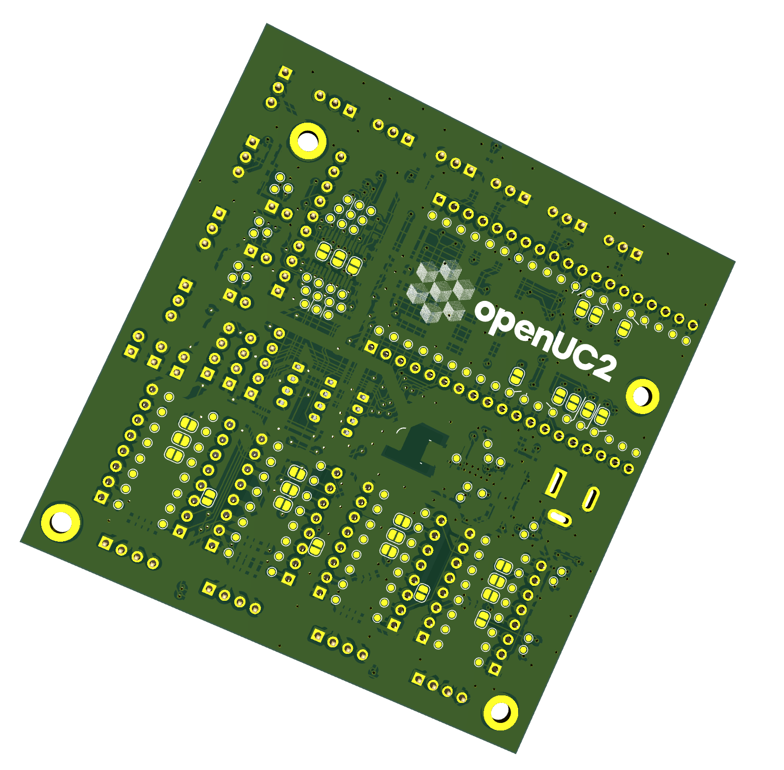
Test pads and solderjumpers
Test pads are on almost every net and are all placed on the bottom side of uc32_standalone. They can be manually probed, soldered to, or probed with a specially designed bed-of-nails (for QA testing). All test points have labels on Silkscreen which can be referenced in the interactive HTML bom, but especially in the schematic.
Solderjumpers can be either open-by-design or closed-by-design. Solderjumpers are not labeled in silkscreen, but they can be identified using the interactive HTML bom. If needed, the gap can be cut with a knife. The gap can also be bridged (again) by making a solder bridge through the gap.
Reset button
The reset button (SW101) in the corner of uc32_standalone is a momentary switch which shorts EN and GND when pushed. This resets the ESP32 board.
The EN pin of the ESP32 board is pulled up on the DEVKIT C module so that the normal state is HIGH, enabling the ESP32 chip.
Errata and notes for the next revision of the board
- The limit switches are not wired how off-the-shelf limit switches are wired commonly.